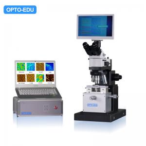
Optical + Atomic Force Microscope, All-in-One
◆ Integrated design of optical metallographic microscope and atomic force microscope, powerful functions
◆ It has both optical microscope and atomic force microscope imaging functions, both of which can work at the same time without affecting each other
◆ At the same time, it has the functions of optical 2D measurement and atomic force microscope 3D measurement
-
◆ The laser detection head and the sample scanning stage are integrated, the structure is very stable, and the anti-interference is strong
◆ Precision probe positioning device, laser spot alignment adjustment is very easy
-
◆ The single-axis drive sample automatically approaches the probe vertically, so that the needle tip is perpendicular to the sample scan
◆ The intelligent needle feeding method of motor-controlled pressurized piezoelectric ceramic automatic detection protects the probe and the sample
-
◆ Ultra-high magnification optical positioning system to achieve precise positioning of probe and sample scanning area
◆ Integrated scanner nonlinear correction user editor, nanometer
-

-
-
-
-
-
-
-
| Specification | A62.4500 | A622.4501 | A62.4503 | A62.4505 |
| Work Mode | Tapping Mode
【Optional】
Contact Mode
Friction Mode
Phase Mode
Magnetic Mode
Electrostatic Mode | Contact Mode
Tapping Mode
【Optional】
Friction Mode
Phase Mode
Magnetic Mode
Electrostatic Mode | Contact Mode
Tapping Mode
【Optional】
Friction Mode
Phase Mode
Magnetic Mode
Electrostatic Mode | Contact Mode
Tapping Mode
【Optional】
Friction Mode
Phase Mode
Magnetic Mode
Electrostatic Mode |
| Current Spectrum Curve | RMS-Z Curve
【Optional】
F-Z Force Curve | RMS-Z Curve
F-Z Force Curve | RMS-Z Curve
F-Z Force Curve | RMS-Z Curve
F-Z Force Curve |
| XY Scan Range | 20×20um | 20×20um | 50×50um | 50×50um |
| XY Scan Resolution | 0.2nm | 0.2nm | 0.2nm | 0.2nm |
| Z Scan Range | 2.5um | 2.5um | 5um | 5um |
| Y Scan Resolution | 0.05nm | 0.05nm | 0.05nm | 0.05nm |
| Scan Speed | 0.6Hz~30Hz | 0.6Hz~30Hz | 0.6Hz~30Hz | 0.6Hz~30Hz |
| Scan Angle | 0~360° | 0~360° | 0~360° | 0~360° |
| Sample Size | Φ≤90mm
H≤20mm | Φ≤90mm
H≤20mm | Φ≤90mm
H≤20mm | Φ≤90mm
H≤20mm |
| XY Stage Moving | 15×15mm | 15×15mm | 25×25um | 25×25um |
| Shock-Absorbing Design | Spring Suspension | Spring Suspension
Metal Shielding Box | Spring Suspension
Metal Shielding Box | - |
| Optical Syestem | 4x Objective
Resolution 2.5um | 4x Objective
Resolution 2.5um | 10x Objective
Resolution 1um | Eyepiece 10x
Infinity Plan LWD APO 5x10x20x50x
5.0M Digital Camera
10" LCD Monitor, With Measuring
LED Kohler Illumination
Coaxial Coarse & Fine Focusing |
| Output | USB2.0/3.0 | USB2.0/3.0 | USB2.0/3.0 | USB2.0/3.0 |
| Software | Win XP/7/8/10 | Win XP/7/8/10 | Win XP/7/8/10 | Win XP/7/8/10 |
-
| Microscope | Optical Microscope | Electron Microscope | Scanning Probe Microscope |
| Max Resolution (um) | 0.18 | 0.00011 | 0.00008 |
| Remark | Oil immersion 1500x | Imaging diamond carbon atoms | Imaging high-order graphitic carbon atoms |
| | |
-
| Probe-Sample Interaction | Measure Signal | Information |
| Force | Electrostatic Force | Shape |
| Tunnel Current | Current | Shape, Conductivity |
| Magnetic Force | Phase | Magnetic Structure |
| Electrostatic Force | Phase | charge distribution |
-
| | Resolution | Working Condition | Working Temperation | Damge to Sample | Inspection Depth |
| SPM | Atom Level 0.1nm | Normal, Liquid, Vacuum | Room or Low Temperation | None | 1~2 Atom Level |
| TEM | Point 0.3~0.5nm
Lattice 0.1~0.2nm | High Vaccum | Room Temperation | Small | Usually <100nm |
| SEM | 6-10nm | High Vaccum | Room Temperation | Small | 10mm @10x
1um @10000x |
| FIM | Atom Level 0.1nm | Super High Vaccum | 30~80K | Damge | Atom Thickness |
-
-
-